Breaking08 / Industry
Samsung reportedly taps TSMC 3nm for Nvidia's NVHBM base die
 Taeoh Kwon· Industry
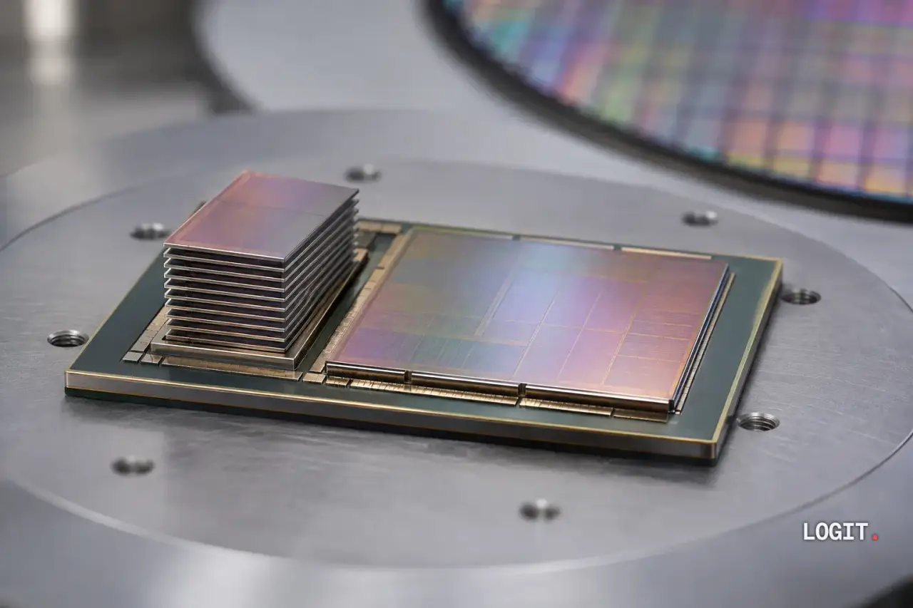
South Korean chipmaker Samsung Electronics has decided to use the 3-nanometre (3nm) process of Taiwan's TSMC for the base die of NVHBM, Nvidia's custom high-bandwidth memory, the business newspaper Seoul Economic Daily reported on 18 Oct 2026.
Nvidia said in August that NVHBM delivers up to 30% more memory bandwidth than standard HBM4E. The design moves the memory controller from the die of the XPU, a custom AI chip, into the HBM base die, the logic layer at the bottom of the memory stack. That frees up to 25% more XPU compute die area than standard HBM4E.
Supply structure. Nvidia said a standard NVHBM implementation will be available from multiple memory providers and that Annapurna Labs, Amazon's chip design unit, will be the first to work on the technology. The Seoul Economic Daily reported that Nvidia had asked Samsung, its South Korean rival SK hynix and US memory maker Micron to standardise base-die processes and core-die specifications. Nvidia's announcement does not name any of the three companies.
Moving the controller into the 3D HBM stack cuts HBM power consumption by 15% compared with standard HBM4E, Nvidia said.
Korean supply chain. In official COMPUTEX 2026 materials, Samsung said it uses its own 4-nanometre (4nm) foundry process for the HBM4E base die and 1c DRAM for the core die. The Seoul Economic Daily reported that Samsung will keep using its own processes for custom products made for customers, which differ from general-purpose HBM.
Samsung and TSMC have not confirmed the use of TSMC's process for the NVHBM base die in an official announcement, and the contract value, yield and unit price have not been disclosed.